ELE447 Spring 1999
A parallel to serial converter is used in many applications. Network Switches rely extensively on these converters as do buses in parallel computers. The utility of a device that can take a barrage of input and organize it in a single file fashion, needs only to be explored to be realized. The layout of the design was small enough, albeit barely, to allow for two implementations of the design on one chip. Ideally three implementations of the design would allow for the realization of the 8 to 1 parallel to serial converter which was our original goal, but this could not be done due to size constraints.
The design is broken up into two parts, an asynchronous input controller, which is Jeremy's part of the design, and a synchronous output controller (SOC), which is Sean's part of the design. The asynchronous input controller (AIC) will control 2 bits of input. In order to get our desired 4 bits of input we used two implementations of the AIC in our design. The original design specification called for 8-bits of input which seriously complicated the job of the SOC. To simplify the job of the synchronous output controller we chose to only implement a 4 to 1 parallel to serial converter(PSC). The 8 to 1 parallel to serial converter could still be implemented with our design if not for size constraints. It would require two copies of the 4 to 1 SPC working in parallel giving us an 8 to 2 SPC. The two outputs could then be placed through another 4 to 1 SPC (although only a 2 to 1 in necessary) to give the desired 1 output.
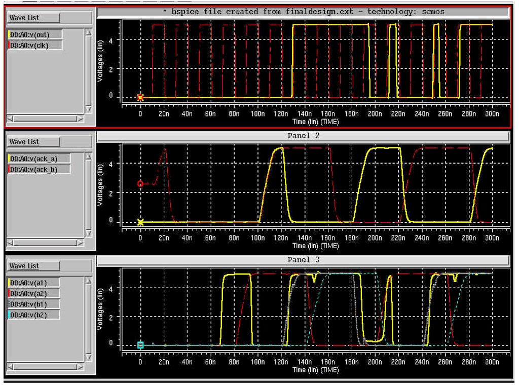
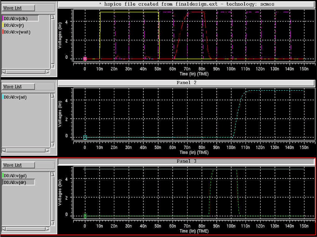
Communication is achieved between the host and AIC, and the AIC and SOC via 4 control signals, DR, ACK, CLEAR, and FULL. The AIC will stay in a "wait" state until the host asserts the DR(data ready) signal. Once the AIC receives an asserted DR signal, the data is read and latched. Once the data is latched, an asserted ACK(acknowledge) signal gets sent back to the host, as well as an asserted FULL(get data) signal being sent to the SOC. The host clears the DR signal once it receives the asserted ACK from the AIC. Data is grabbed from the SOC, shifted out , and then the SOC sends an asserted CLEAR signal to the host and AIC, which proceeds to the "wait" state.
Several pins are for debug purposes only. Pins A1Out, A2Out, B1Out,and B2Out, for both chip implementations are debug pins used for testing. Each chip implementation must be treated separately. Each will require its power, gnd, and inputs, and will provide its own output.
PIN SPECIFICATIONS:
| Chip Implementation One | Chip Implementation 2 |
| 1 | A1Out | 18 | B2Out |
| 40 | A2Out | 19 | B1Out |
| 39 | B1Out | 20 | A2Out |
| 38 | B2Out | 21 | A1Out |
| 2 | Out | 22 | Out |
| 3 | Reset | 23 | Reset |
| 4 | CLK | 24 | CLK |
| 5 | VDD | 25 | VDD |
| 6 | Data Input 2, B Input | 26 | Not used |
| 7 | Data Input 1, B Input | 27 | Data Input 1, Input B |
| 8 | ACK, B Input | 28 | Data Input 2, Input B |
| 9 | Data Ready, B Input | 29 | ACK, Input B |
| 10 | Data Input 2, A Input | 30 | Data Ready, Input B |
| 11 | Data Input 1, A Input | 31 | Data Input 2, Input A |
| 12 | ACK, A Input | 32 | Data Input 1, Input A |
| 13 | Data Ready, A Input | 33 | ACK, Input A |
| 14 | Not used | 34 | Data Ready, Input A |
| 15 | GND | 35 | GND |
| 16 | Not used | 36 | Not used |
| 17 | Not used | 37 | Not used |
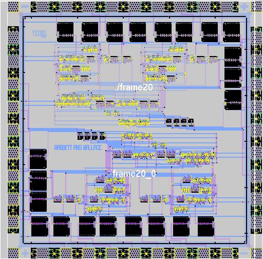
Chip Layout:
4 to 1 Parallel to Serial Converter:
CLK = Clock.
OUT = The output
ACK_A = Acknowledge signal for input A
ACK_B = Acknowledge signal for input B
A1, A2, B1,and B2 = Inputs
ASYNCHRONOUS INPUT CONTROL:
CLK = Clock
R= Reset Signal
WAIT= Wait State
AD = Acknowledge Data Signal
DR = Data Ready Signal
GD = Get Data Signal
TEST 1:
Power Consumption Test.:
This is the simplest and the most important of all the tests. This will check to see
if any shorts were created during the manufacturing.
1. Hook up VDD to 5 volts and GND to ground.
2. Connect an ammeter or multimeter between the VDD and the power supply
3. The current drawn should be on the order of milliamps.
4. Repeat test for the second chip implementation.
TEST 2:
AIC Test:
This test will check to see if the AIC responds to the assertion of the DR signal from the
host.
1. Connect VDD to 5 volts and GND to ground.
2. Use a function generator to create a square wave with a 10Mhz frequency and 5
volt amplitude. Connect that signal to CLK.
3. Assert the RESET pin for a time period greater than the clock. (100 ns).
4. Clear the RESET pin.
5. Connect DATA INPUT 1, A INPUT and DATA INPUT 2, A INPUT to ground.
6. Assert DATA READY, A INPUT.
7. Check the ACK, A INPUT pin. The signal should be high.
(asserted)
8. Repeat test for input "B".
9. Repeat test for the second chip implementation.
TEST 3:
SOC Shift Response Test:
This test will check to see if the SOC is shifting out data in the proper order.
1. Connect VDD to 5 volts and GND to ground.
2. Use a function generator to create a square wave with a 10Mhz frequency and 5
volt amplitude. Connect that signal to CLK.
3. Assert the RESET pin for a time period greater than the clock. (100 ns).
4. Clear the RESET pin.
5. Connect DATA INPUT 1, A INPUT and DATA INPUT 2, A INPUT to ground.
6. Assert DATA READY, A INPUT.
7. Check the ACK, A INPUT pin. The signal should be high.
(asserted)
8. Clear DATA READY, A INPUT.
9. Watch A1OUT, and A2OUT. A1OUT should become high for one clock cycle before
returning low. The next clock cycle A2OUT should become high for
one clock cycle before returning low.
10. Check the ACK, A INPUT pin. This signal should be low (cleared)
11. Repeat test substituting input "A" for input "B".
12. Repeat test for the second chip implementation.
TEST 4:
Functionality Test:
This test will check whether or not the Parallel to Serial Converter performs its task.
1. Connect VDD to 5 volts and GND to ground.
2. Use a function generator to create a square wave with a 10Mhz frequency and 5
volt amplitude. Connect that signal to CLK.
3. Assert the RESET pin for a time period greater than the clock. (100 ns).
4. Clear the RESET pin.
5. Connect DATA INPUT 1, A INPUT, DATA INPUT 2, A INPUT, DATA INPUT 1, B
INPUT, and DATA INPUT 2, B INPUT to an arbitrary combination of highs and lows.
(ex DATA INPUT 1, A INPUT and DATA INPUT 2, B INPUT to 5 Volts, and DATA INPUT 2, A
INPUT and DATA INPUT 1, B INPUT to 0 volts).
6. Assert DATA READY, A INPUT, and DATA READY.
7. Check the ACK, A INPUT and ACK, B INPUT pins. The signals
should be high. (asserted)
8. Clear DATA READY, A INPUT and DATA READY, B INPUT.
9. Watch OUT. The signal should appear the same as your inputs in the
order DATA INPUT 1, A INPUT, DATA INPUT 2, A INPUT, DATA INPUT 1, B INPUT, and
DATA INPUT 2, B INPUT.
10. Repeat test for the second chip implementation.
The first, and most startling, conclusion that can be made is that the chip is easily filled. It had been surmised that this design would be very small and only cover a small corner of the chip, but that was not the case. The layout was large enough that two implementations of the design could barely fit on the chip and still allow for enough room to buffer the inputs and outputs. It is easy to see why much of the design process is spent doing the layout. With a simple design, testing quickly becomes difficult. The reason for this is partly because of all of the possibilities for error created during fabrication of the chip. That is why simple tests like the Power Consumption Test, are so important and can save a lot of time.