The contact on the p-side is 2 microns from the junction. The contact on the n-side is 10 microns from the junction. The junction area is 10 microns by 10 microns.
- What is the built in potential?
Vbi = VT ln[NAND / ni2] = 0.877V
- What is the position of the Fermi level relative to the
intrinsic level on the n side of the junction?
Ef - Ei = VT ln[ND /ni] = 0.365V
- What is the value of the saturation
current, Is, in the equation,
I = Is*eV/Vt
Is = A q ni2 Dp / ND Wn = 1.8 x 10⁻¹⁷ A
where, Dp = VT up = 0.0259*440
-
Draw the equilibrium energy band
diagram for this junction, including numerical
values for the Fermi level position relative
to the intrinsic level on each side.
Show the built-in potential on the diagram.
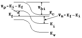
Vn = 0.365 eV, Vp = 0.51 eV, Vbi = 0.87 eV