
Introduction:
The reason for using CMOS (Complementary Metal Oxide Semiconductor) technology today is to improve the leading-edge products in terms of cost, density, speed and power. For example, specialized fabrication companies are able to reduce the feature size (wire size) from 10m m (micrometer) all the way down to 0.25m m. This allows designers to develop multifunction designs that fit on a signal chip. As a result, the cost, size, and power consumption are reduced but the products’ speed is increased. Some examples of the utilization of feature size reduction are: PC’s (which are running anywhere from 50MHz all the way to 500MHz), laptop computers as strong as the PC’s but portable, cellular phones which fit in your hand and a normal digital watch that also has the functions of a beeper. Therefore, the integration of circuitry onto a single package has become of extreme importance. Such integration has spawned families of design, namely: SSI (small-scale integration), MSI (medium scale integration), LSI (large-scale integration), VLSI (very large scale integration) and, recently, ULSI (ultra large-scale integration). It is primarily VLSI systems that are addressed within this project.
Design Description:
The following design incorporates a binary coded decimal (BCD) to seven-segment display decoder with drivers. The drivers are used to amplify the digital signal that is outputted from the BCD, basically allowing the output to be clean enough to be displayed on the 7-segment displays. It should be noted that, if the input were not in BCD format, undesirable output such as hexadecimal numbers would be displayed. Furthermore, one can externally input 8-bit binary code, whose higher nibble (first 4-bits: A3, A2, A1, A0) represents the "ten’s" place of a decimal number and whose lower nibble (last 4-bits: B3, B2, B1, B0) represents the "one’s" place of a decimal number. In addition, four 2 to 1 multiplexers are used to select whether the higher or lower nibble will be passed to the BCD to seven-segment decoder. The same select input used for the multiplexers is utilized in the operation of the demuxiplexer. Demuxiplexer’s individual outputs, D1 and D0, are externally connected to R1 and R2 resistors which are wired to the base of two separate NPN transistors (2N3904). These two NPN transistors have their emitter connected to the ground and their collector attached to the seven-segment display’s common cathode pins. The mentioned "select" input, which for this design is synonymous with "CLK", can be manually inputted using a DIP switch or utilizing a function generator. Such a feature allows the user to display data that changes with time as it appears at the input. Also, the displays can be tested by using DIP switches as a manual input of 16 different two 4-bit binary combinations, and then manually selecting which display is to show the higher or lower nibble.
To further increase the utility and testability of the chip, a pair of static decade counters is also included. With each clock transition, one counter is responsible for counting from 0 to 9 for the "one’s" place. This counter will trigger the secondary counter, which will count from 0 to 9 for the "ten’s" place. This occurs when the "1001" state is present in the first counter. To exclude the "A" through "F" states, both counters have a feedback network that resets the counters when the "1010" state is reached. The result is a display, which counts from 0 to 99 that can be used as needed by the user or simply as a means of testing the chip’s operation. Therefore, the chip has two modes of operation: counter mode and external data mode. Eight tristate gates, which were created from scratch, control these two modes. By varying the logic at the DTNCNTEN pin, one can enable the counters and disable the external data flow if the logic is zero (0 volts); otherwise, to disable the counters and enable the external data flow, one should apply logic one (5 volts) to the pin.
Truth Table for the BCD:
|
INPUTS |
OUTPUTS |
|||||||||||
|
Decimal/Hex |
D |
C |
B |
A |
a |
b |
c |
d |
e |
f |
g |
|
|
0 |
0 |
0 |
0 |
0 |
1 |
1 |
1 |
1 |
1 |
1 |
0 |
|
|
1 |
0 |
0 |
0 |
1 |
0 |
1 |
1 |
0 |
0 |
0 |
0 |
|
|
2 |
0 |
0 |
1 |
0 |
1 |
1 |
0 |
1 |
1 |
0 |
1 |
|
|
3 |
0 |
0 |
1 |
1 |
1 |
1 |
1 |
1 |
0 |
0 |
1 |
|
|
4 |
0 |
1 |
0 |
0 |
0 |
1 |
1 |
0 |
0 |
1 |
1 |
|
|
5 |
0 |
1 |
0 |
1 |
1 |
0 |
1 |
1 |
0 |
1 |
1 |
|
|
6 |
0 |
1 |
1 |
0 |
1 |
0 |
1 |
1 |
1 |
1 |
1 |
|
|
7 |
0 |
1 |
1 |
1 |
1 |
1 |
1 |
0 |
0 |
1 |
0 |
|
|
8 |
1 |
0 |
0 |
0 |
1 |
1 |
1 |
1 |
1 |
1 |
1 |
|
|
9 |
1 |
0 |
0 |
1 |
1 |
1 |
1 |
1 |
0 |
1 |
1 |
|
|
10 = A |
1 |
0 |
1 |
0 |
1 |
1 |
1 |
0 |
1 |
1 |
1 |
|
|
11 = b |
1 |
0 |
1 |
1 |
0 |
0 |
1 |
1 |
1 |
1 |
1 |
|
|
12 = C |
1 |
1 |
0 |
0 |
1 |
0 |
0 |
1 |
1 |
1 |
0 |
|
|
13 = d |
1 |
1 |
0 |
1 |
0 |
1 |
1 |
1 |
1 |
0 |
1 |
|
|
14 = E |
1 |
1 |
1 |
0 |
1 |
0 |
0 |
1 |
1 |
1 |
1 |
|
|
15 = F |
1 |
1 |
1 |
1 |
1 |
0 |
0 |
0 |
1 |
1 |
1 |
|
The above BCD’s truth table is implemented into a bcdmux.pla file. The conversion program optimizes the design even more than using a simplified Boolean equation. By using the Boolean equation method, one will get 38 sum-of-products that are derived by the compiling program. On the other hand, using the bcdmux.pla, the truth table gives a sixteen sum-of-products. This really reduces the size of the circuit and increases the operation speed. After the file bcdmux.pla is created, one needs to go to the UNIX prompt and type " mpla –s SCS3cis bcdmux.pla ". The compiling program at that time will generate a file called bcdmux.mag. Checking the current directory, one needs to see if the bcdmux.mag file exists. If it does not exist, look at the filename.pla and redo the steps again. This process is very useful for optimization. The bcdmux.pla file is shown below
Bcdmux.pla file:
.i 4
.o 7
.ilb D C B A
.ob a b c d e f g
.p 16
|
0 |
0 |
0 |
0 |
1 |
1 |
1 |
1 |
1 |
1 |
0 |
|
|
0 |
0 |
0 |
1 |
0 |
1 |
1 |
0 |
0 |
0 |
0 |
|
|
0 |
0 |
1 |
0 |
1 |
1 |
0 |
1 |
1 |
0 |
1 |
|
|
0 |
0 |
1 |
1 |
1 |
1 |
1 |
1 |
0 |
0 |
1 |
|
|
0 |
1 |
0 |
0 |
0 |
1 |
1 |
0 |
0 |
1 |
1 |
|
|
0 |
1 |
0 |
1 |
1 |
0 |
1 |
1 |
0 |
1 |
1 |
|
|
0 |
1 |
1 |
0 |
1 |
0 |
1 |
1 |
1 |
1 |
1 |
|
|
0 |
1 |
1 |
1 |
1 |
1 |
1 |
0 |
0 |
1 |
0 |
|
|
1 |
0 |
0 |
0 |
1 |
1 |
1 |
1 |
1 |
1 |
1 |
|
|
1 |
0 |
0 |
1 |
1 |
1 |
1 |
1 |
0 |
1 |
1 |
|
|
1 |
0 |
1 |
0 |
1 |
1 |
1 |
0 |
1 |
1 |
1 |
|
|
1 |
0 |
1 |
1 |
0 |
0 |
1 |
1 |
1 |
1 |
1 |
|
|
1 |
1 |
0 |
0 |
1 |
0 |
0 |
1 |
1 |
1 |
0 |
|
|
1 |
1 |
0 |
1 |
0 |
1 |
1 |
1 |
1 |
0 |
1 |
|
|
1 |
1 |
1 |
0 |
1 |
0 |
0 |
1 |
1 |
1 |
1 |
|
|
1 |
1 |
1 |
1 |
1 |
0 |
0 |
0 |
1 |
1 |
1 |
.e
Probably one might think, "what do these terms mean?" Well don’t worry. Here is the list of definitions.
·
.i 4 à ( .i ) indicates the input and the number 4 tells how many inputs there are.·
.o 7 à ( .o ) represents the output and the number 7 tells how many outputs there are.·
.ilb and .ob à allows one to label inputs and outputs for easy identification.·
.p 16 à ( .p ) stands for sum-of-products (SOP) and the number 16 allows to modify the minimum SOP terms that are based on the truth table.·
Truth table à make sure that there is a space between the input and output of the binary code sequence.·
.e à refers to the end of file.After finishing, save the file as some_filename.pla and make sure that the file has an extension of .pla.
The 2 to 1 multiplexer, demultiplexer, and the feedback network for the counters were done in a similar way as stated above. Thus, there are other ways of obtaining designs besides using the Uricells library. Each component was tested individually and was proven to work. Then the individual pieces were connected together. Tests show that the unit as whole functions properly.
Objective:
This design can be used in conjunction with other circuits that are required to display binary codes in decimal format. Some examples would be: a digital thermometer that outputs a binary result, a Microwave oven display, an advance version of a reflex response circuit, a display for the digital odometer/speedometer of an automobile, and other gadgets that need this functionality. It only takes imagination to develop other uses for this chip. Primarily, it is a practical circuit that has the flexibility to incorporate with other designs.
Schematics:
In this section, one will see a Block Diagram of this design, and two Electronic Work Bench’s (EWB) gate level schematics. The Block Diagram gives a general overview of the circuit and identifies various functions. EWB layout #1 shows the tristate gate implementation with external data and counter inputs that share the four 2 to 1 multiplexers. This sketch also includes the demultiplexer, DTNCNTEN (data not counter enable) pin, and the CLK (clock/manual input) pin. EWB layout #2 exhibits the BCD to 7-segment display with the drivers (buffers).
BLOCK DIAGRAM
The above diagram demonstrates several functions that allow the counter or the external data to be displayed in a decimal format, so the user can easily understand the binary input. The static counters were downloaded from the Uricells library, and these counters can be identified by looking at the filename.mag, which includes the "st" (For example, counter5st.mag is a static counter). The reason for this type of counter is that the overall function of the design operates at low frequencies (so that one is able to read each individual number on the displays). For higher frequencies, one would use a dynamic counter. These counters have no "st" in their filename.mag (For instance, counter5.mag is a dynamic counter). Furthermore, the difference between the dynamic and static components is that at low switching frequencies, the static power dissipation is most important, but at higher switching rates, the dynamic components become dominant.
EWB LAYOUT #1
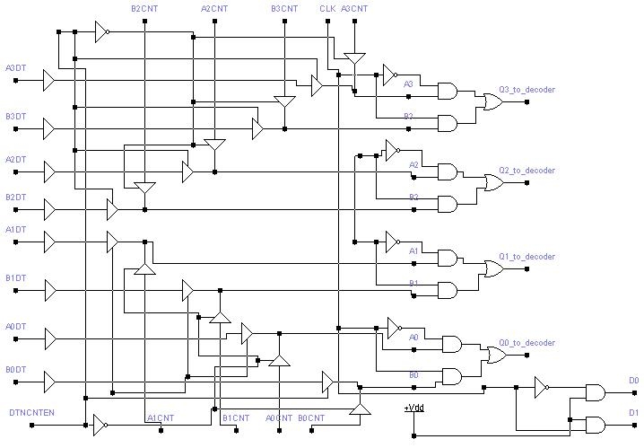
Looking at the EWB layout #1, one will see inputs ending in DT. The DT indicates external data inputs. Anything ending in CNT signifies counter inputs. The counters were not used in this schematic layout because they were downloaded from the Uricells library and tested separately by using Hspice simulator.
EBW LAYOUT #2
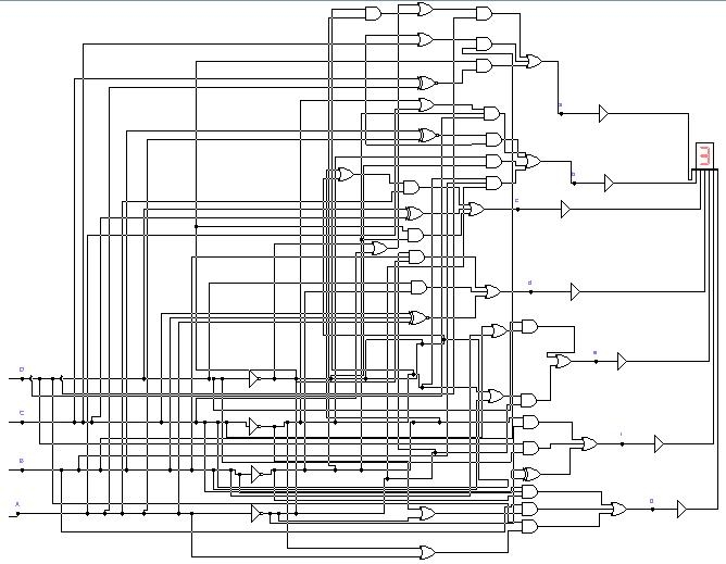
By deriving the Boolean equation from the BCD’s Truth Table, EWB Layout #2 was created. The following equations are for the BCD:
·
a = !D&((!A&!C)|(A&C))|B&(C|!D)|D&(!A|(!B&!C))·
b = (!C&!D)|!D&((A&B)|(!A&!B))|!B&D&(A|!C)·
c = ((!C&D)|(C&!D))|(A&!B)|(!B&!D)|(A&!D)·
d = (!&!B&!C)|(A&B&C)|(!A&B&!D)|(!A&B&C)|(!B&D)·
e = !A&(B|!C)|D&(B|C)·
f =(!A&!B)|((C&!D)|(!C&D))|(B&D)·
g = (!B&C&!D)|B&(!A|!C)|D&(A|!C)·
‘&’ à Stands for logical ‘AND’ operation;·
‘|’ à Logical ‘OR’ operation;·
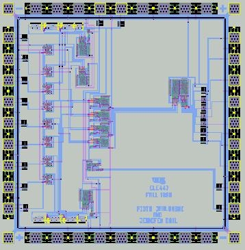
‘!’ à Logical ‘NOT’ operation;VLSI LAYOUT
The below VLSI layout will be in the fabricated chip.
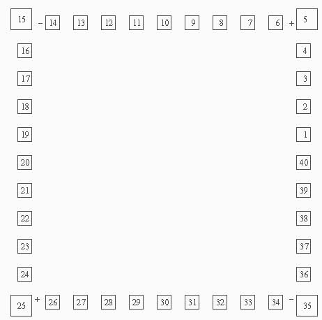
PIN Diagram of the VLSI Layout:
Reserved pins are #5 and #25 for Vdd, and #15 and #35 for GND.
Hspice Simulation Results:
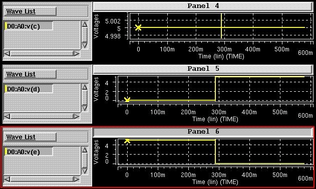
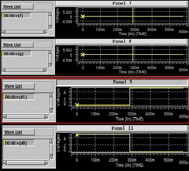
In order to interpret the Hspice results from the wave form diagrams below, one needs to refer to the corresponding "Table for External Data Mode" and the " Table for Counter Mode". After selecting the time limits, one would read from the top to the bottom in the time range that is chosen for each individual signal (square wave). These tables will help one to understand the complexity of the pictures with ease. The word "TOP" will be used to indicate the beginning of the mode and the word "BOTTOM" will refer to the end of the mode. Time is represented in milliseconds (ms).
Table for External Data Mode:
|
Time in ms |
CLK |
a |
b |
c |
d |
e |
f |
g |
D1 |
D0 |
Decimal or Hex |
||
|
0 -- 290 |
0 |
1 |
1 |
1 |
0 |
1 |
1 |
1 |
0 |
1 |
A |
||
|
290 -- 580 |
1 |
1 |
0 |
1 |
1 |
0 |
1 |
1 |
1 |
0 |
5 |
TOP of External Data Mode:
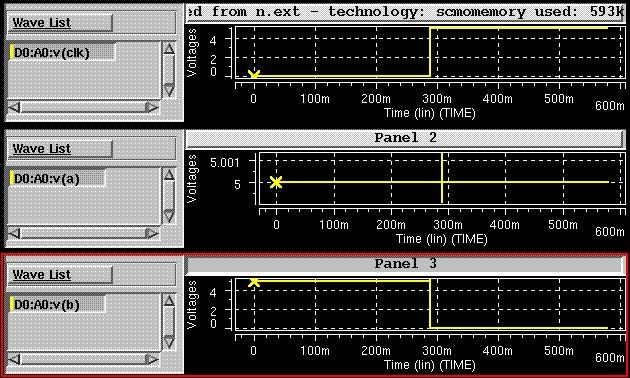
Bottom of External Data Mode:
Table for the Counter Mode:
|
Time in ms |
CLK |
a |
b |
c |
d |
e |
f |
g |
D1 |
D0 |
Decimal or Hex |
||
|
0 -- 20 |
1 |
1 |
1 |
1 |
1 |
1 |
1 |
0 |
0 |
1 |
0 |
||
|
20--40 |
0 |
1 |
1 |
1 |
1 |
1 |
1 |
0 |
1 |
0 |
0 |
||
|
40--60 |
0 |
1 |
1 |
1 |
1 |
1 |
1 |
0 |
0 |
1 |
0 |
||
|
60--80 |
0 |
0 |
1 |
1 |
0 |
0 |
0 |
0 |
1 |
0 |
1 |
||
|
80--100 |
0 |
1 |
1 |
1 |
1 |
1 |
1 |
0 |
0 |
1 |
0 |
||
|
100--120 |
0 |
1 |
1 |
0 |
1 |
1 |
0 |
1 |
1 |
0 |
2 |
||
|
120--140 |
0 |
1 |
1 |
1 |
1 |
1 |
1 |
0 |
0 |
1 |
0 |
||
|
140--160 |
0 |
1 |
1 |
1 |
1 |
0 |
0 |
1 |
1 |
0 |
3 |
||
|
160--180 |
0 |
1 |
1 |
1 |
1 |
1 |
1 |
0 |
0 |
1 |
0 |
||
|
180--200 |
0 |
0 |
1 |
1 |
0 |
0 |
1 |
1 |
1 |
0 |
4 |
||
|
200--220 |
0 |
1 |
1 |
1 |
1 |
1 |
1 |
0 |
0 |
1 |
0 |
||
|
220--240 |
0 |
1 |
0 |
1 |
1 |
0 |
1 |
1 |
1 |
0 |
5 |
||
|
240--260 |
0 |
1 |
1 |
1 |
1 |
1 |
1 |
0 |
0 |
1 |
0 |
||
|
260--280 |
0 |
1 |
0 |
1 |
1 |
1 |
1 |
1 |
1 |
0 |
6 |
||
|
Time in ms |
CLK |
a |
b |
c |
d |
e |
f |
g |
D1 |
D0 |
Decimal or Hex |
||
|
280--300 |
0 |
1 |
1 |
1 |
1 |
1 |
1 |
0 |
0 |
1 |
0 |
||
|
300--320 |
0 |
1 |
1 |
1 |
0 |
0 |
1 |
0 |
1 |
0 |
7 |
||
|
320--340 |
0 |
1 |
1 |
1 |
1 |
1 |
1 |
0 |
0 |
1 |
0 |
||
|
340--360 |
0 |
1 |
1 |
1 |
1 |
1 |
1 |
1 |
1 |
0 |
8 |
||
|
360--380 |
0 |
1 |
1 |
1 |
1 |
1 |
1 |
0 |
0 |
1 |
0 |
||
|
380--400 |
0 |
1 |
1 |
1 |
1 |
0 |
1 |
1 |
1 |
0 |
9 |
||
|
400--420 |
0 |
0 |
1 |
1 |
0 |
0 |
0 |
0 |
0 |
1 |
1 |
||
|
420--440 |
0 |
1 |
1 |
1 |
1 |
1 |
1 |
0 |
1 |
0 |
0 |
||
|
440--460 |
0 |
0 |
1 |
1 |
0 |
0 |
0 |
0 |
0 |
1 |
1 |
||
|
460--480 |
0 |
0 |
1 |
1 |
0 |
0 |
0 |
0 |
1 |
0 |
1 |
||
|
480--500 |
0 |
0 |
1 |
1 |
0 |
0 |
0 |
0 |
0 |
1 |
1 |
||
|
500--520 |
0 |
1 |
1 |
0 |
1 |
1 |
0 |
1 |
1 |
0 |
2 |
||
|
520--540 |
0 |
0 |
1 |
1 |
0 |
0 |
0 |
0 |
0 |
1 |
1 |
||
|
540--560 |
0 |
1 |
1 |
1 |
1 |
0 |
0 |
1 |
1 |
0 |
3 |
Top of the Counter Mode:
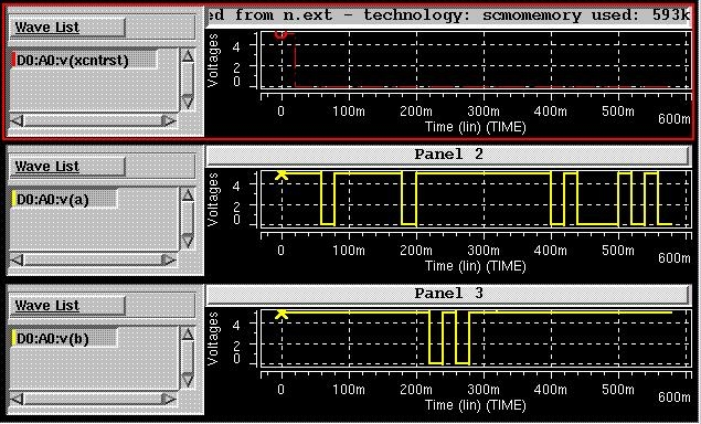
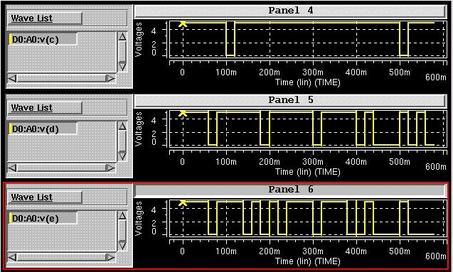
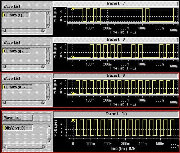
Bottom of the Counter Mode:
PIN LAYOUT:
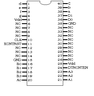
PIN CONNECTION and PROCEDURE:
·
Connect all NC pins, pin #15, and pin #35 to GND; pin #5 and pin #25 to 5 volts (Vdd).·
CLK is pin #10. This pin can be used as a manual input of logic 1 or 0. Also one can connect this pin to an external function generator (input a square wave). For the counter one can use the frequency range 4 to 10Hz in order to read the display normally, but for extreme fast speed use any frequency ranging from 10Hz to 1KHz. In the name of science, try varying the frequency range to see which frequency is proper.·
DTNCNTEN is pin #24. The pin means Data Not Counter Enable. By applying logic 1 (5volts), external DATA is allowed to go through and using logic 0 (0 volts) the COUNTER is enabled.·
XCNTRST is pin #11. This pin is used for external counter reset. Prior to using the counter, apply logic 1 (5 volts) to reset the counter and then change the logic back to 0 (0 volts) in order for the counter to continue to count from 0 to 99. If left alone, the counter will continue to cycle through the numeric sequence from 0 to 99.·
B3 & A3 are considered as MSB (Most significant bits) and B0 & A0 are considered as LSB (Least significant bits).These pin assignments are used for external data:
|
Chip's pins |
1's place |
Chip's pins |
10's place |
|
16 |
B0 |
20 |
A0 |
|
17 |
B1 |
21 |
A1 |
|
18 |
B2 |
22 |
A2 |
|
19 |
B3 |
23 |
A3 |
Pin Layout of 7-segment display for NTE3056, NTE3058, NTE3059, or NTE3060.
|
Chip's pins |
Anode |
7-segment display pins |
|
1 |
d |
7 |
|
2 |
e |
6 |
|
3 |
f |
1 |
|
4 |
g |
2 |
|
38 |
a |
14 |
|
39 |
b |
13 |
|
40 |
c |
8 |
·
Both of the 7-segment displays share the same output from the chip. Between the chip’s outputs and the two 7-segment display inputs, one needs to connect seven 220W resistors. Refer to diagram below: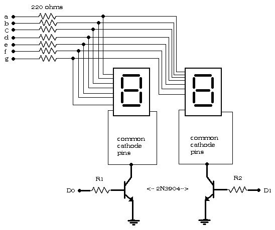
·
Common Cathode Pins are #4 and #12. For more detailed information about the above 7-segment displays go to http://www.nteinc.com/specs/3000to3099/NTE3056.html . The 10’s place Common Cathode Pins need to be wired to the Collector of the 10’s place NPN transistor (2N3904). The 1’s place Common Cathode Pins need to be connected to the Collector of the 1’s place NPN transistor (2N3904). To see the pin layout of the 2N3904 transistor go to http://www.uoguelph.ca/~antoon/gadgets/2n3904.jpg·
To determine the values for R1 and R2, look at the Data Sheet of 2N3904 transistor to find the allowed base current (IB). Measure the voltage drop from chip’s pins D1 and D0, and then use Ohm’s Law (R=(V/I)) to find the resistor. Experimental values of V=5volts and I<1mA were used. Therefore, this gave a resistor value of R=5.6KW for R1 and R2, which should be a sufficient value for testing. WARNING— By not using resistor values for R1 and R2, the transistors will be destroyed.·
D1 is pin #37. This pin needs to be wired to the R2 resistor that is connected to the base of a NPN transistor, which controls the 1’s place.·
D0 is pin #36. This pin needs to be wired to the R1 resistor that is connected to the base of a NPN transistor, which controls the 10’s place.·
Anode D.P. is pin #9. This pin is your basic Decimal Point on the 7-segment display. To connect it is optional.Conclusions:
One can see the benefits of integration with this BCD to seven-segment decoder/driver/counter design. If one were to try to implement this design by connecting gates on a circuit board, the result would be quite cumbersome. Furthermore, from this circuit design one develops a better understanding of the CMOS construction as well as making system level design decisions. As with any undertaking, problems arose. Such problems included input file error and extraction failure. The input file error was corrected by going back to the Magic Program, and erasing all labels. After this was done, the labels were renamed and then the layout was resaved. It seems that there was a problem with the link between the current project directory and the Uricells library. It would seem that the files associated with the components of the library would be extracted with the entire design; however, this was not the case. By removing all files corresponding to the given layout (except for the files with the *.mag extensions), and copying the required files from Uricells library to the current directory, the extraction failure was eliminated. As demonstrated, simulations showed a functional design. Therefore, if the chip is tested properly within the given specifications, any failures should be assumed to come from the fabrication process. Therefore, it is very important to double check the pin connections and make sure everything is hooked up correctly.