|


|

|
|

ELE405 Digital Computer Design (3)
Hardware implementation of digital computers. Arithmetic circuits, memory
types and uses, control logic, basic computer organization, microprogramming,
input/output circuits, microcomputers.
(Lec. 3) Pre: (301, 305, and (credit or concurrent enrollment in 406)) or permission of instructor.
ELE 406 Digital Computer Design Lab (1)
Laboratory exercises related to topics in 405.
(Lab. 3) Pre: credit or concurrent enrollment in 405.
|
Course Description: After completing this course, you should
understand how a computer system is built and how it operates from the
viewpoints of the computer architect, the assembly language programmer, and
the logic designer. You will learn how to design the internal components of
a processor, including the datapath and control unit, the arithmetic logic
unit, and the memory system. You also will develop an understanding of the
performance and implementation trade-offs inherent in any computer design.
Laboratory:
The main tool for this class is the Altera’s Quartus II.
Visit Altera's website for a free Quartus II web edition which runs on
any typical PC (Windows and Linux versions are both available). Quartus II is a
comprehensive package includes schematic editor, state diagram editor, VHDL
entry and synthesis tool, DSP
design tools and utilities, and FPGA implementation and configuration.
There will be eight scheduled laboratories
to practice some advanced topics in CPU and computer system designs.
Project:
There is a semester project for ELE405.
Students will first design and implement their CPUs from scratch. At the
second stage of the project, students are expected to build
prototypes of real-life computer-based systems using their own CPUs.
|
|
|
|
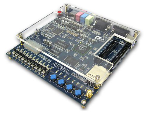
The main hardware facility is the DE1 board from Terasic. It carries a
Altera's Cyclone II EP2C20 FPGA in a 484-pin package. This FPGA has 18,752
programmable logic elements, 239,616 on-chip RAM bits, 52 embedded 9-bit
multipliers, and four phase locked loops (PLLs).
The FPGA configuration file is downloaded from
the host computer via Altera's USB Blaster.
|
|
Time
& Location:
Lectures:
TTh 11:00-12:15 pm, Kelley 102.
Labs:
section 1: M 2:00 - 4:45 pm, Kelley 220.
section 2: T 2:00 - 4:45 pm, Kelley 220.
Instructor:
Dr. Jien-Chung Lo
- Office: Kelley Annex 221
- Phone: x4-2996
- Email: jcl@ele.uri.edu
- Office Hours: W 1-3PM and Th 2-3PM
ELE406 Teaching Assistant:
Mr. Daxian Yun
- Office: Kelley 211
- Email: dyun@ele.uri.edu
- Office hours: TBA
|
|