Department of Electrical and Computer Engineering
![]() University
of Rhode Island
University
of Rhode Island
Department of Electrical and Computer Engineering
Section 2: Mentor Graphics IC Station Layout Tutorial
In this section you will use IC Station to create the Layout for the CMOS inverter. The Layout will use Cherry Semiconductor's PS3 process and PS3 layout rules.
1) Invoke IC Station
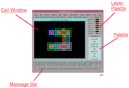
If needed, start the Design Manager (DM) by typing "dmgr" at the command line. When the DM window appears, use the MGC > Location Map > Set Working Directory menu item to change to the ~/inv directory that you created in Section 1. Start IC Station by double clicking the "ic" button in DM's Tools Window. IC Station should now appear on the desktop. Some of the important windows in IC station are highlighted below. Note that neither the Cell Window nor the Layer Palette will be visible when IC Station first starts.
2) Create a new cell
Create a new cell using the File > Cell > Create pull-down menu, or you can also click the "Create" button on the Palette. A Create Cell dialog box will appear.
In the Cell Name box, enter ~/inv/inv_cell. This will create the cell in the inv directory with the name inv_cell.
In the Process box, use the navigator to choose the file: /ocean/research/cherry/process/PS3_200-034. This file describes the PS3 process.
In the Rules box, use the navigator to choose the file: /ocean/research/cherry/rules/PS_3_RULES. This file describes the layout rules for the PS3 process.
Click OK
A blank Cell window will open up.
3) Show Layer Palette
Displaying the Layer Palette will make the layout procedure much easier.
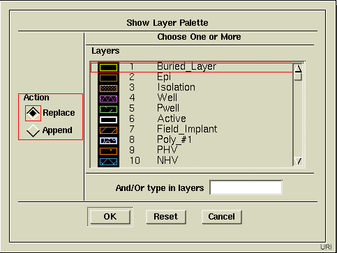
With the IC Station window active, type in the command "sho la palette". As you type a command window will appear like the one pictured below.
Hit enter to execute the command.
The Show Layer Palette Selection box will appear. Hold down the control key to select layers 1, 2, 5, 6, 11, 13, 15, 16, 18, 19, and 95. We will use these layers to create the inverter.
(Show Layer Palette Box)
When you click OK, the Layer Palette will appear in the IC window with all the selected Layers. Note: Sometimes when the Layer Palette is visible, not all the Palette commands are visible. You can right click on the Palette to show scrollbars for the window.
4) Lay out the inverter shapes and masks.
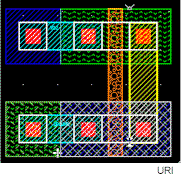
Once the Layer Palette is visible you can lay out the inverter. Use the Easy Edit menu on the Palette to create the shapes and masks for the layout. If you have trouble creating the shapes for the different layers, see the IC User's Manual Tutorial in the Bold Browser (type "bold_browser" at the command line). A completed inverter layout can be seen here. Please note the specific details for the PS3 process, if some of these details are missed, the LVS link in section 3 may not work.
5) Add Text to the VCC and GROUND Nets
Add text to the Metal_#1 shapes that represent the VCC and GROUND pins.
Type the command "add text" or right click on the layout and use the Add > Text menu item.
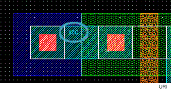
Add a text item with the value "VCC" to the VCC net (as shown below), make sure the text falls within the VCC metal_#1 shape. Also, make sure that the text object is a metal_#1 object. You can change the text object's layer by highlighting the text, and typing "cha la".
follow the same procedure to add "GROUND" text to the GROUND net.
6) Check for errors
IC Rules must be run manually to check for design rules errors. To run IC Rules, click on "IC Rules" in the Palette, then Click on "Check". IC Rules will display messages in the message bar as it runs. When IC rules is complete, the following message will appear in the message bar:
The "Total Results", in this case 3, indicates the number of design rule errors in your layout. To view the errors one by one, use the "First" and "Next" buttons in the Palette. As shown here, each error will be highlighted individually and a description of the error will be displayed in the message bar. Fix all errors in the layout so that the "Total Results" of the IC Rules check is 0.
7) Creating Ports
Ports (or pins) are the inputs and outputs of your cell. They define the functional interface for the cell component. For the inverter, you must define 4 ports: in, out, VCC, and GROUND.
Use the Context > Set Cell Config > Connectivity Editing... menu item to switch the cell to connectivity mode.
Highlight the "out" port as shown below:
Use the Objects > Ports: > Make Port menu item to create the port. A dialog box like the one below will appear in the IC Station window:
Change the value of the Direction box to display "out" and name the port "OUT" - Click OK.
Repeat this procedure for the three remaining ports. The port parameters are summarized here.
Return to geometry editing by using the Context > Set Cell Config > Geometry Editing... menu Item.
The inverter cell layout is now complete. Save the cell and close the inverter Cell Window.
8) Create an LVS Cell
In order to link the cell using Layout vs. Schematic (LVS - Section 3), we need to create a second cell and add a few more layers.
- Create a new cell as described in step 2 of this tutorial, but name the cell inv_cell_lvs.
- Use the Easy Edit -> Cell button on the palette to add an inverter to the new layout. In the window that appears, type in "~/inv/inv_cell" to add the inverter. Use the mouse to place the inverter cell in the center of the screen. You should see a cell representation of the inverter you created, but only the four ports are visible. If you want to see more of the inverter cell layers then highlight the cell object, and type "peek" or "peek 99". As you peek a layer or a range of layers it will become visible.
- To complete the LVS inverter cell, you need to add three things: A Buried Layer, an Epi layer, and LVS Text with the value "10V". The LVS Text must be inside the epi layer, it must be layer 95 (LVS_TEXT layer), and it must be all capital letter.The final layout for the LVS cell can be seen here.
- Use IC Rules to fix all errors and save the cell.
That's all for Section 2,
Go on to Section 3: LVS Tutorial
Mentor Graphics Tutorial Home Page
Created by: Seth
Milman, 6/27/98
Last Modified: 7/2/98